
Prev
Investment Highlights
1. Domestic substitution has evolved from an investment theme to formal production schedules. The White Paper on High‑Speed Optical Module Industry Development, released by the MIIT on June 26, 2026, stipulates that newly built 10k‑GPU‑scale intelligent computing centres must be equipped with 800G/1.6T optical modules, while 400G and lower‑speed products are removed from procurement lists. It also sets a quantified target for the self‑sufficiency rate of high‑end 200G EML optical chips to reach 45% by 2028. Policy has laid out the timeline; the key differentiator now lies in reliable on‑time delivery.
2. Value is shifting from manufacturing to design and packaging. Rather than focusing solely on module vendors, track two core metrics: optical chip self‑sufficiency and overseas capacity deployment. Midstream optical modules form the narrow waist of the industry hourglass (typical foundry gross margin: 15%–25%; leading players with in‑house chip development: 30%–40%). Profit upside is primarily driven by localized optical chips, which represent the genuine pricing power at this bottleneck segment.
3. The most certain segments are often not the most hyped ones. Silicon photonics, whose penetration is expected to exceed 50% in 2026, serves as the common foundation across all technical routes. CW lasers are the fundamental utility for the CPO era. These two areas carry higher certainty than debates over individual competing architectures.
4. Map out time windows clearly. LPO has a usable window of only 5–7 years; large‑scale CPO commercialization will arrive in 2027–2028; 3.2T products will not hit peak deployment until 2029–2030. Early investment does not guarantee successful returns; exit timing must align with mass commercial adoption.
5. Key risks require proactive hedging: slower‑than‑expected rollout of CPO/NPO, longer service life of pluggable modules than projected, stretched valuations among leading firms, and recurring overseas sanctions and substitution dynamics.
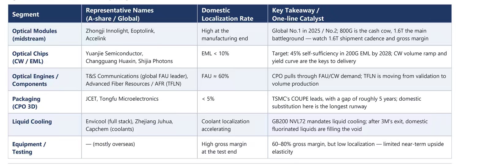
Disclaimer: The covered stocks are an illustrative pool for the segments mentioned herein, for research framework only and do not constitute investment advice.
Part 1 Physical Bottlenecks: Why Light Has Become the Main Battlefield
1.1 Fundamentals of Optical Communication: Transmitting Data with Light Instead of Electricity
An optical fiber is an extremely thin glass or plastic core that confines and transmits optical signals via the principle of total internal reflection of light within the core. Compared with copper cables, optical fibers offer two major advantages. First, they deliver massive bandwidth capacity. Thanks to the high frequency of optical carriers, a single optical fiber supports far higher channel capacity than copper wires. Second, transmission loss is low. The attenuation of modern single-mode fiber can reach roughly 0.2 dB/km, requiring fewer relay amplification nodes for long-distance transmission.
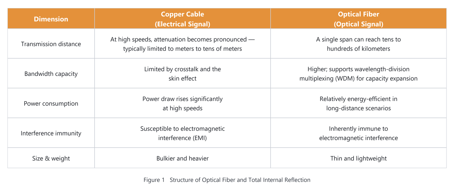
A typical point-to-point optical communication link consists of a transmitter, a receiver and transmission medium. The transmitter modulates electrical signals into optical signals and couples them into the optical fiber. After the optical signals travel through the fiber to the far end, the receiver detects and converts them back into electrical signals.

Optical Module Industrial Chain
The optical module industrial chain is a vertically divided system with optical chips and electrical chips as the core upstream, precision packaging and manufacturing as the midstream, and communication equipment vendors and cloud providers as downstream. Technical barriers and value distribution vary markedly across segments.
• Core upstream components fall into two categories: optical chips (lasers, detector chips) and electrical chips (DSP, laser drivers, transimpedance amplifiers / TIAs). Together they account for over 60% of the bill-of-material cost of an optical module, representing the segment with the highest technical barriers and concentrated value. Other components such as optical assemblies (lenses, isolators, FAU fiber arrays), PCB substrates and metal mechanical parts have relatively lower entry thresholds, yet their requirements for precision and thermal dissipation keep rising for high-speed applications.
• The midstream covers optical module packaging and manufacturing. Vendors integrate upstream components into standardised modules including SFP, QSFP-DD and OSFP via high-precision surface mounting, active/passive coupling, hermetic packaging and burn-in testing. This segment serves as a critical link connecting upstream and downstream.
• Downstream participants include communication equipment suppliers, telecom carriers and leading internet / cloud computing firms. Their capital expenditure and technology roadmap directly shape the iteration pace of optical module specifications. The rapid upgrade of AI data centres from 400G to 800G and further to 1.6T is currently driving prosperity across the whole industrial chain.

1.2 Start with One Curve: Computing Power Doubles While Interconnect Scales Up
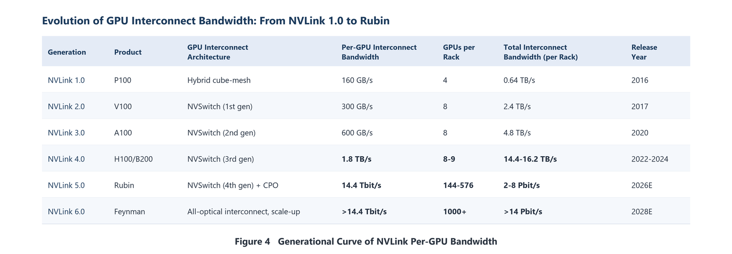
NVLink is NVIDIA’s proprietary high-speed GPU interconnect technology, now in its sixth generation. It delivers a per-GPU bandwidth of 3,600 GB/s (NVIDIA official figure: twice the prior generation and over 14× that of PCIe Gen6, quoted as aggregated bidirectional bandwidth). Based on generational stacking estimates, per-GPU NVLink bandwidth has risen roughly 90× over eight years. Meanwhile, the number of GPUs per rack has climbed from around 4 to 576 (approximately 144×; 576 GPUs correspond to next-generation form factors such as Rubin Ultra NVL576, while the current mainstream NVL72 configuration uses 72 GPUs). Multiplying the two metrics, total rack-level interconnect bandwidth has surged by over ten thousand times (roughly 13,000×) across the eight-year window.
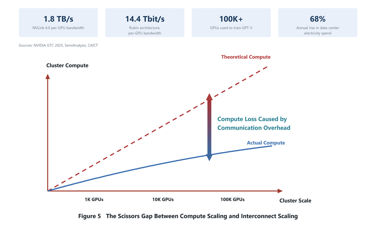
The essence of large-model training lies in distributed computing. According to reverse engineering estimates by SemiAnalysis, GPT-4 adopts an MoE architecture with approximately 1.8 trillion parameters (not officially confirmed by OpenAI). Its training cluster deployed around 25,000 A100 GPUs and took roughly 90–100 days. Tensor parallelism requires frequent data exchange between chips; whenever a GPU sits idle waiting for data, massive capital investment is left underutilized.
The core tension is this: computing power doubles year on year, while interconnect speeds advance only by generation. Interconnect has become a direct constraint on the linear scaling of usable cluster compute capacity — this is the fundamental reason why optical technology has evolved from a peripheral component into the main battlefield of AI infrastructure over the past two years.
1.3 Three Hard Limits of Copper: Bandwidth, Latency and Power Consumption
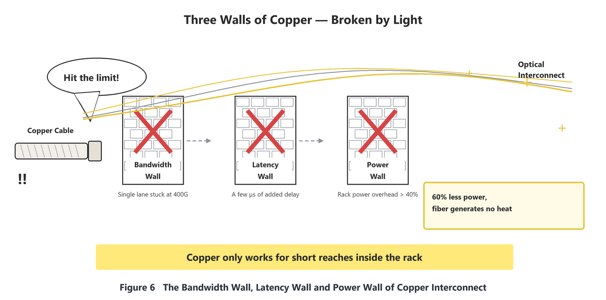
Traditional copper interconnects are hitting three bottlenecks simultaneously.
Bandwidth limit: Single-lane speeds struggle to break 400 Gbps. The skin effect and dielectric loss of copper render high-speed signals barely usable over distances beyond 1 meter. Quantitative reference: an 800G passive copper cable (DAC) incurs 8–12 dB loss at 1 meter. On the logarithmic dB scale, 3 dB corresponds to half the power.
Latency limit: Copper links introduce transmission latency of several microseconds, which multiplies during collective communication in ten-thousand-GPU clusters.
Power consumption limit: This is the most underappreciated bottleneck. At speeds above 200 Gbps, interconnect systems account for over 40% of data centre electricity bills, and rack-level interconnect power consumption exceeds 40%. Secondary effects compound the problem: copper cables are conductors. At 200 Gbps, a 1-metre copper cable carries a transmission loss of roughly 1–3 W per link. Hundreds of thousands of links in a ten-thousand-GPU cluster translate into tens of megawatts of heat load. Once the server room temperature rises, cooling consumes an additional 30%–40% of IT equipment power. Optical fibre itself generates almost no heat from signal transmission and does not require dedicated cooling (note: “no heat generation” refers to heat from transmission loss relative to copper cables; connectors and optical modules still require thermal management). Under equivalent conditions, optical interconnects can cut interconnect power draw by approximately 60%.
One counterintuitive point must be noted: copper will not disappear. For short-reach applications within racks, at board level and below 1 metre, copper remains the lowest-cost, lowest-power and lowest-latency option.
Part 2 Competition Among Technology Routes: CPO / NPO / Silicon Photonics / TFLN
2.1 Composition of Optical Modules: A High‑Booming Track Amid the AI Compute Arms Race
An optical module is a highly complex optoelectronic conversion device precisely integrated from five core components: optical chips, electrical chips, PCB substrates, structural housings and optical assemblies. At the optical transmitter end, laser chips convert high-speed electrical signals into modulated optical signals under the control of driver chips.
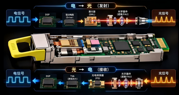
At the optical receiving end, the photodetector chip (PD) captures optical signals and converts them into weak electric currents. The signals are then shaped and amplified by a transimpedance amplifier (TIA) and a limiting amplifier. For high-speed scenarios, the digital signal processor (DSP) handles complex modulation, demodulation and signal compensation. As the most value-concentrated segments, optical and electrical chips together account for over 60% of the bill-of-material cost and directly determine the module’s data rate, power consumption and transmission reach. Serving as the electrical interconnection carrier, the PCB substrate connects chips with external circuits via high-density traces, while delivering stable impedance control and power distribution for high-frequency signals.
Optical assemblies consist of precision components such as lenses, optical isolators, optical filters and FAU fiber arrays. They perform optical coupling, collimation, wavelength division and signal transmission, with assembly precision often reaching micron or even sub-micron levels. The structural housing provides mechanical support and environmental protection, and integrates heat sinks and electromagnetic shielding. These five categories of components are densely packed into a compact form factor via standardized packaging including SFP, QSFP-DD and OSFP. As data rates evolve from 800G to 1.6T, device density and thermal stress rise simultaneously.
2.2 NPO and CPO: Moving the “Translator” Inside the Chip
Conventional pluggable devices act like external translators: data exits the GPU, travels over copper wires to the optical module, and is then converted into optical signals. Every step consumes power and introduces latency and noise.
CPO follows a straightforward approach: the optical engine and switch chip are packaged on the same substrate, with optical signals routed directly adjacent to the chip and eliminating all intermediate interfaces. The analogy is shifting simultaneous interpretation from “an interpreter sitting at the back with a microphone” to “real-time interpretation right beside your ear”.
NPO serves as an intermediate and often underappreciated milestone on this roadmap. The optical engine and packaged XPU are placed side-by-side on the same high-performance PCB within a few centimetres, with channel loss capped below 13 dB and interconnect density 2–3 times higher than pluggable solutions. It delivers two practical advantages. First, high GPU temperatures do not directly impact temperature-sensitive optical components, preventing wavelength drift. Second, if the optical section fails, only the optical engine module needs replacement, without touching the entire packaged unit.
These two merits make NPO the primary technical route adopted by domestic GPU chip vendors at present.
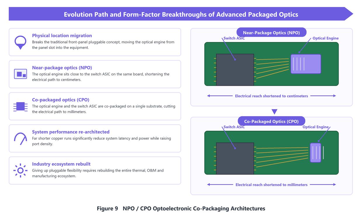
CPO will not “kill off” pluggable modules. According to Yole, Nomura and LightCounting estimates: CPO penetration stood below 3% from 2024 to 2026; it will reach 10%–15% during 2027–2028; and approach 30% in data‑centre switching applications after 2029, while pluggable solutions (traditional, LPO and XPO combined) will still account for roughly 70% of the market.
2.3 Generational Shift of Data Rates
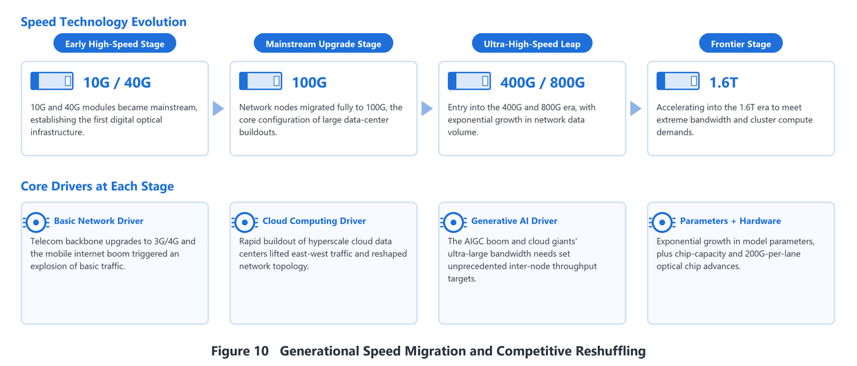
The doubling of optical module data rates with each new generation has been the most consistent industrial trend over the past decade. It brings three outcomes: higher average selling prices (ASP), a window of high gross margins, and reshuffling of the competitive landscape. Generational transitions follow a well-established empirical rhythm: volume ramp-up begins in the first year after commercial launch, peak deployment occurs in Years 2–3, the generation is superseded by the next one in Years 3–4, and it is removed from new procurement lists in Years 4–5.
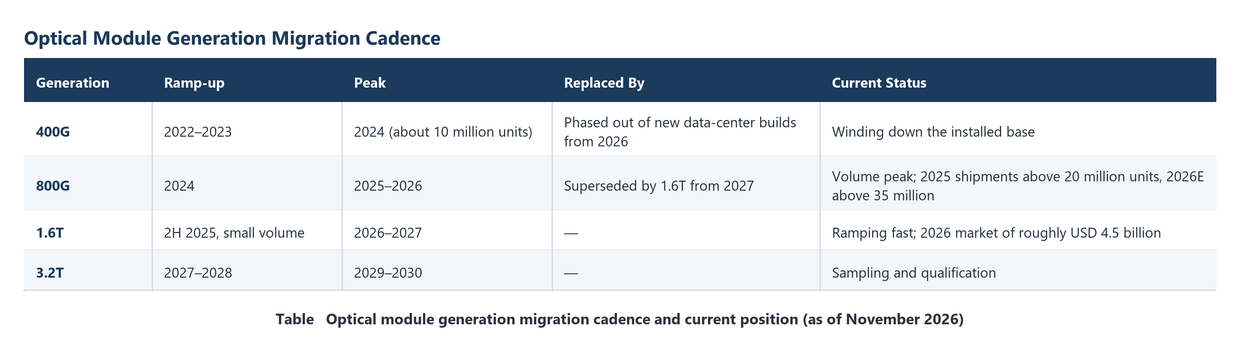
High-speed optical modules have gone through four generations of rate jumps, evolving from early 10G/40G to 100G, then to 400G/800G, and now advancing toward 1.6T. This evolution is driven jointly by traffic growth and technological progress: earlier iterations were fueled by telecom upgrades and cloud computing traffic, while the current wave is strongly propelled by exploding parameter sizes of large AI models, higher switching chip capacity, and breakthroughs in 200G per wavelength transmission. To sum up: 800G is today’s cash cow, 1.6T is next year’s main battlefield, and 3.2T represents the option for the year after next.
2.4 Silicon Photonics: Standout High Integration and Scalable Manufacturing Potential
Beneath all competing technical routes lies a more fundamental certainty: silicon photonics. As a foundational technology for high-density, high-speed and energy-efficient optical interconnects, silicon photonics not only underpins optical modules but also enables more advanced NPO and CPO architectures. Its core value lies in leveraging CMOS-compatible processes to integrate optical signal generation, transmission, modulation and detection, alongside optical and electronic components, onto a single silicon chip.
Benefiting from the cost advantages, mature processes and manufacturability of silicon, silicon photonics combines the precision and scalability of IC fabrication with the high-speed and low-power merits of photonics. It addresses the drawbacks of traditional discrete optoelectronic components, including high costs, low integration and excessive power consumption. Multiple research institutes project silicon photonics module penetration to exceed 50% in 2026, making it the most robust long-term growth track.
2.5 Thin-Film Lithium Niobate (TFLN): The Performance Leader for Next-Gen Ultra-High-Speed Modulation
Thin-film lithium niobate is essentially conventional lithium niobate, a well-established electro-optic crystal, thinned down to nanoscale thickness (analogous to shaving a thick plank into thin paper). It retains the material’s inherently superior electro-optic properties while enabling mass production via semiconductor processes, just like silicon photonics. If InP represents the “present” for optical chips and silicon photonics the “near-term future”, TFLN is the “longer-term future” and one of the highest-performance solutions for the 1.6T/3.2T era.
Thin-Film Lithium Niobate (TFLN) vs. Silicon Photonics vs. Indium Phosphide (InP):
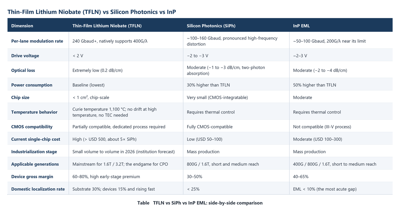
TFLN does not replace InP or silicon photonics; instead, it fills the gap for ultra-high-speed modulation within the optical chip material ecosystem. Global demand for 1.6T optical modules is ramping rapidly in 2026 (LightCounting estimates: 14–25 million units). Traditional silicon photonics and InP EMLs are approaching physical limits for long-reach 1.6T applications. By contrast, TFLN delivers high bandwidth (the AM70 supports 70 GHz per lane, and higher-bandwidth coherent-driven modulators are undergoing customer validation), making it one of the commercially available solutions natively supporting modulation above 200G per wavelength.
Public information shows that the AM70 thin-film lithium niobate modulator from Aofar Photonics entered volume shipment in March 2025. Its 96 Gbaud / 130 GBaud coherent-driven modulators are also on the validation or mass-production rollout lists of leading optical module vendors. Jinan Jingzheng supplies 3/4/6-inch single-crystal lithium niobate thin films, while yields for 6-inch wafers are still climbing. On the cost side, a standalone TFLN modulator currently costs more than US$500. With the migration from 6-inch to 8-inch substrates and automated packaging, the target cost is US$150–200 by 2028, at which point its cost-performance will match silicon photonics alternatives.
2.6 Liquid Cooling: The “Air Conditioner” for CPO
CPO presents an almost counterintuitive physical dilemma: switch chips consume over 1,000 W, comparable to a small electric heater, while the adjacent lasers must operate stably at 25 ℃ ± 0.1 ℃. Temperature fluctuations exceeding 0.1 ℃ may trigger wavelength drift and communication outages, which air cooling cannot resolve. Liquids carry roughly 20 times the heat capacity and have a thermal conductivity around 25 times that of air. NVIDIA GB200 NVL72 (with rack power consumption above 120 kW) mandates liquid cooling, with direct-to-chip cold plates as the official reference design. This requirement carries over to the subsequent GB300 NVL144. Major OEMs are expected to shift fully to liquid-cooled shipments in 2026.
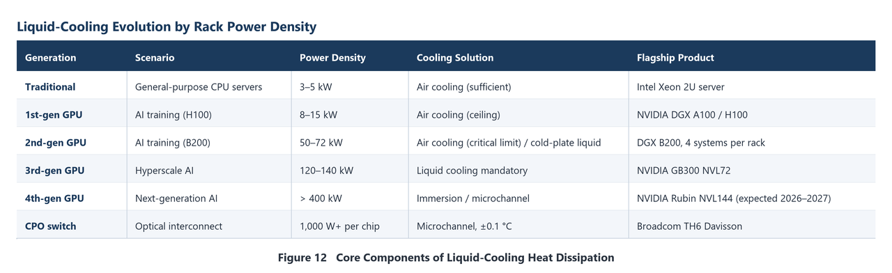
The combined 2026 market size for the four core components — CDU, cold plates, quick-disconnect fittings and coolant — is approximately RMB 26.5 billion, capturing the lion’s share of profit across the industrial chain. The larger midstream system integration segment (around RMB 30.5 billion) faces sustained margin compression from downstream price pressure.
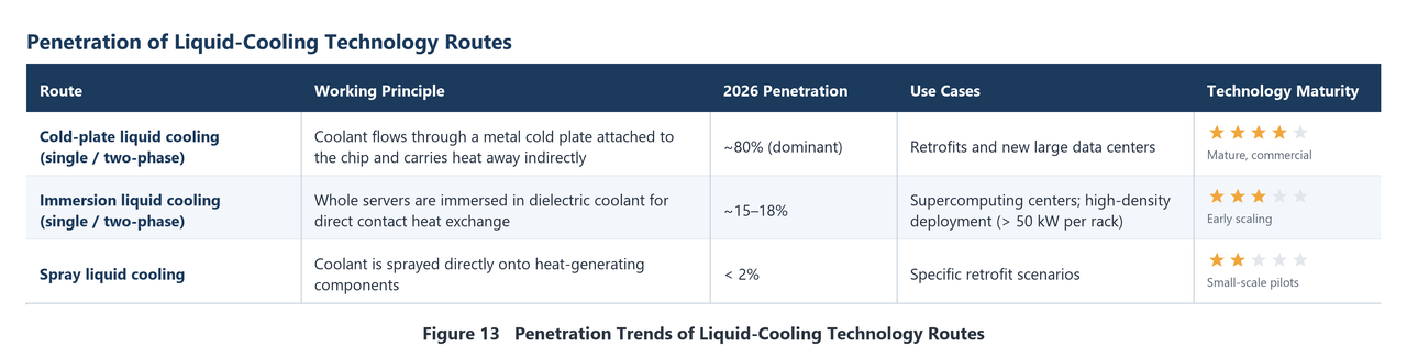
Trend 1: Cold-plate cooling remains the dominant architecture from 2025 to 2028 (80% → 65% → 50%), with its share declining gradually. It offers better compatibility for both retrofits and new builds alongside lower TCO.
Trend 2: Immersion cooling will see accelerated penetration starting in 2028. Cold-plate solutions cannot deliver sufficient cooling efficiency once single-chip TDP exceeds 1,500 W, making immersion the only viable option.
Trend 3: Domestic substitution for cooling fluids is speeding up. Following 3M’s exit from the global electronic fluorinated fluid market, Juhua Co., Ltd. (600160) and New Zhubang (300037) are filling the gap.
Trend 4: End-to-end delivery is emerging as a prevailing model, shifting from component sales to full solution offerings. Envicool’s full-stack strategy has proven advantageous.
Trend 5: AI-powered intelligent liquid cooling, which dynamically adjusts flow rate and temperature based on real-time power consumption forecasting, is expected to push PUE further below 1.05.
Part 3 Value Distribution and Bottlenecks: Where the Profit Pools Lie at Both Ends
3.1 Hourglass-Shaped Value Distribution
The optical interconnect industry features a classic hourglass value structure. Upstream optical chips carry gross margins of 50%–80%, and downstream test equipment reaches 60%–80%. The midstream optical module segment forms the narrow waist of the hourglass: conventional foundry and low-value-added modules deliver gross margins of roughly 15%–25%, while leading in-house chip developers achieve materially higher levels. For example, Innolight posted an optical module gross margin of approximately 34.6% in 2024, with overall gross margin ranging from 34% to 37%.
Based on its 2025 annual report, Innolight recorded revenue of RMB 38.24 billion and net profit attributable to parent of RMB 10.797 billion, representing a net profit margin of around 28.2%. Full domestic localization of optical chips could lift its net margin to 35%–40%. This represents the largest profit upside across the whole chain and reflects the genuine pricing power behind this critical bottleneck.
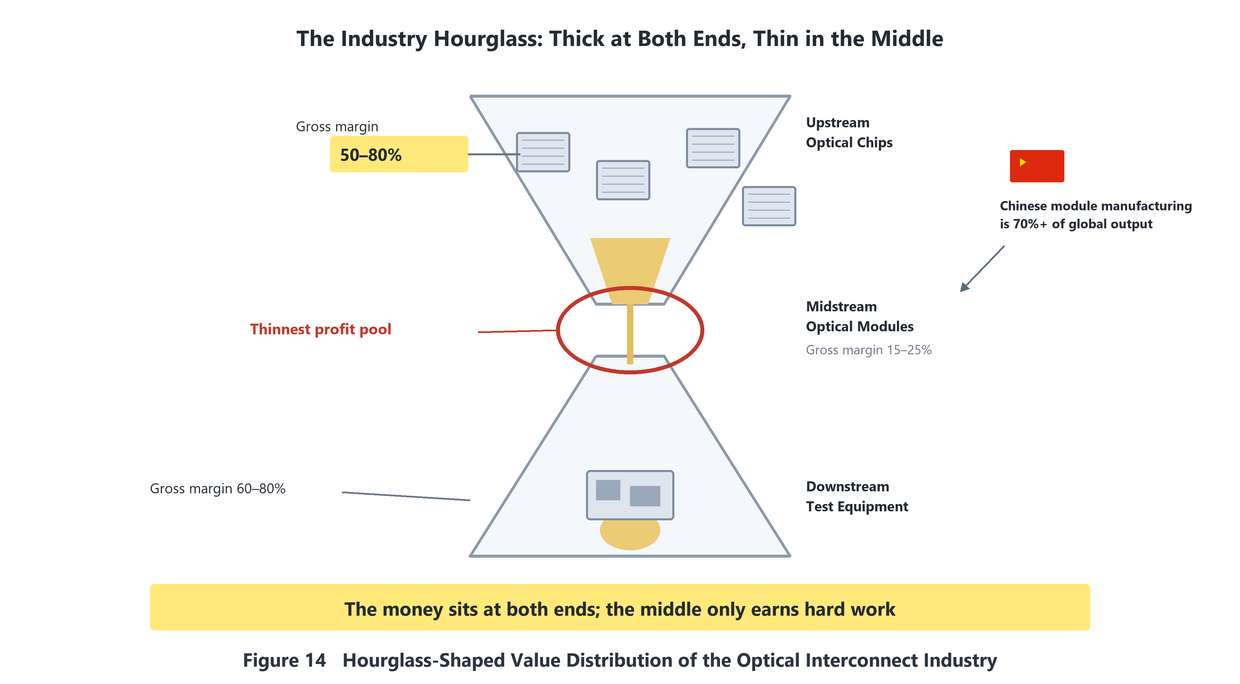
The current landscape is as follows: Chinese vendors collectively hold more than 60% of the global optical module market share (with an even higher share in manufacturing). The global optical module market grew by 58% in 2025, with Innolight ranking first and Eoptolink second worldwide. According to the LightCounting May 2026 ranking, seven Chinese suppliers are among the global Top 10 (Innolight, Eoptolink, Accelink, Nazhen Technology, Huagong Genuine, Source Photonics, and Cambridge Technology). Nevertheless, the domestic self-sufficiency rate for upstream EML laser chips stands below 10%–25% (the self-sufficiency rate for high-end EML chips above 100G is merely in the single digits), while the self-sufficiency rate for DSP chips is less than 10%.
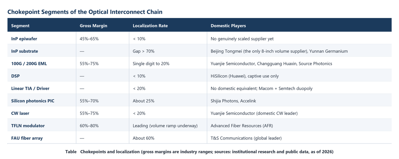
3.2 Bottleneck List: Unpacking the Profit Pools
A breakdown of core bottlenecks reveals where the value resides:
3.3 Structural Opportunity: CW Lasers
One standout structural opportunity from the list merits separate discussion: CW lasers. Under CPO/NPO architectures, light sources are decoupled from modulation. CW lasers only generate light, while modulation is handled by modulators integrated on silicon photonic chips. Silicon is poor at light emission yet excels at modulation and waveguide functions; CW lasers fill this sole gap in the silicon photonics ecosystem.
According to the prospectus of Yuanjie Semiconductor, global CW laser chip sales reached approximately USD 0.04 billion in 2024, are projected to hit USD 0.2 billion in 2025, and may exceed USD 10 billion by 2030 (implying a CAGR of roughly 150%). The CW light source market is set for a CAGR of around 121% from 2024 to 2027 (reaching about USD 0.767 billion in 2027). High-power CW lasers rated above 100 mW boast an even higher CAGR of approximately 276% over 2024–2030, with the 100 mW+ CW market expected to reach USD 6.6 billion in 2030. Separately, estimates from Yunling Optoelectronics’ prospectus put China’s optical chip market size at nearly RMB 9 billion in 2025, forecast to rise to RMB 19.4 billion by 2029.
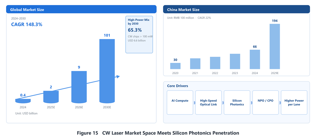
CW lasers represent one of the sub‑segments where the gap between leading domestic players and overseas suppliers is the narrowest. Yuanjie Semiconductor shipped more than 1 million CW light sources in 2024 and posted revenue of approximately RMB 601 million in 2025 (+140% year‑on‑year), with an overall gross margin of around 58%. Its 300 mW CW laser matches the performance of comparable Coherent products, with progress now constrained by yield ramp‑up. Once it crosses the roughly 70% yield threshold, Yuanjie will become one of the few manufacturers worldwide capable of mass production alongside Coherent.
Part 4 Investment Risks
1. Technology roadmap timing risk: If the large‑scale commercial rollout of CPO/NPO (expected for 2027–2028) is delayed, or pluggable solutions (traditional + LPO + XPO) enjoy longer service life than forecast, overextended valuations of CPO‑related names may reverse.
2. Demand and capital expenditure risk: A marginal slowdown in AI capex by overseas cloud vendors could weaken shipment momentum and ASP upside for 1.6T/800G modules.
3. Valuation and crowding risk: Leading players (Innolight, Eoptolink) trade at elevated valuations after explosive earnings growth in 2025. Volatility driven by over‑optimistic expectations and crowded positioning warrants caution.
4. Supply chain and geopolitical risk: Domestic self‑sufficiency for high‑end EML/DSP optical chips remains low. Tighter overseas export controls may disrupt deliveries; US market access and tariff policies are subject to change.
5. Yield delivery risk: The upside of bottleneck‑breakthrough stocks such as Yuanjie’s CW lasers and Aofar’s TFLN hinges fundamentally on scheduled yield improvements and mass production ramp. Failure to deliver would invalidate the investment thesis.
6. Competitive landscape risk: While the midstream module sector is concentrated, the transition to 1.6T TFLN and silicon photonics brings risks of market share reshuffling and misplaced technology bets.
Appendix: Data Sources & Notes
LightCounting (May 2026 Top 10 optical module ranking), Yole Group, Omdia, Cignal AI, SemiAnalysis, TrendForce; public materials from Broadcom, Arista and NVIDIA; Research Report on the Development and Application of Information Photonics Technology (2025) by CAICT; White Paper on Optical Interconnect Technologies for Large‑Scale Intelligent Computing Clusters (2025) by China Mobile Research Institute; White Paper on High‑Speed Optical Module Industry Development (MIIT, June 26, 2026); Innolight 2024/2025 annual reports; Yuanjie Semiconductor prospectus and public disclosures; research reports from Guosen Securities, Great Wall Securities, Zheshang Securities and Soochow Securities.
 Jumbo Sheen Fund
Disclaimer:The content involved in this article is for sharing and exchange purposes only, and shall not be construed as investment advice. It is provided merely for readers' reference. All copyrights of the quoted content belong to the original authors. If any infringement is found, please contact us for removal.